Sidebar
Table of Contents
5.8 GHz Frequency-Hopping Signal Generator
During the summer of 2012, I took a microwave design lab class. The main project was to design a frequency-hopping microwave signal generator. Although the device wouldn't actually modulate any data, it would have to send a continuous wave (CW) signal on a frequency, then hop to the next frequency. The device had to be Part 15 FCC compliant. The device also had to be milled on our school's machine, which meant the board would be made of FR4 and copper.
Project Requirements
- Operation within the 5.725 – 5.850 GHz ISM (unlicensed) band; no measurable out-of-band signal
- +7 dBm of output power (5 mW)
- Uses at least 75 frequency channels, spaced 1 MHz apart
- Maximum 0.4s dwell time on 1 carrier frequency during a 30s interval
- Self-contained design on a single circuit board
A high-level diagram of the signal generator was also provided:
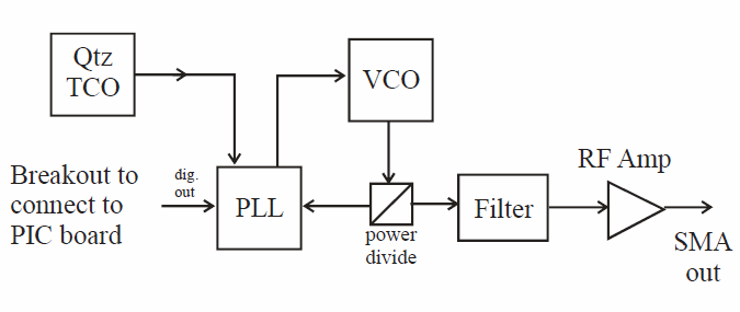
The carrier wave was to be generated by a voltage-controlled oscillator (VCO), which is controlled via a feedback loop with a phase-locked loop (PLL) IC. The frequency set-point of the PLL is programmable via SPI connection to a microcontroller, which will provide the frequency-hopping functionality. A crystal oscillator provides a 10 MHz reference signal for the PLL. Finally, the VCO output will be filtered through a band-pass filter to remove any out-of-band components, and an RF amplifier will boost the signal to the desired 7dBm output power.
Components
The following components were specified by the professor:
| Component | Manufacturer | Part Number |
|---|---|---|
| Quartz Oscillator | Fox Electronics | FXO-HC536R-20 |
| 3.3 V Voltage Regulator | Diodes Inc | AP1117E33GDIDKR |
| 5.0 V Voltage Regulator | Fairchild Semiconductor | LM7805CT-ND |
| PLL Synthesizer | Analog Devices | ADF4107BRUZ |
| Voltage-Controlled Oscillator | Mini-circuits | ROS-5776-119+ |
| Broadband RF Amplifier | Mini-circuits | GALI-39+ |
| Microcontroller | Microchip | PIC18F2321 |
A PhD student was supposed to provide a MSP430 dev board we would be using for control, but I convinced my group to use a PIC instead. I already had experience with PICs and figured it would be faster for me to use a micro I'm already familiar with - plus I was able to put it on the same PCB, whereas other groups used some wires to connect their board to an MSP430 dev board. It turned out using the PIC was a smart idea, since the MSP430 dev board proved to be quite challenging for the other groups.
PLL Design
The PLL was implemented using the reference circuit provided in the ADF4107 datasheet, shown below:
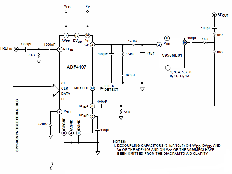
In PLL design, the critical component to design is the loop filter. There are two key parameters of the PLL that would have an impact on loop filter design: loop bandwidth and phase margin. The loop bandwidth influences the lock time. In the project requirements, the maximum lock time is 0.4s. This is a very long time, and normally a transmitter would use most of this time to actually send data. The PLL should be able to lock within 100us. Based on this requirement, the loop bandwidth is set to 50KHz. The simulation indicated that the lock time is only 40us, which meets our requirement. The calculations and simulations were performed with ADIsimPLL.
Wilkinson Power Divider
The PLL requires feedback from the VCO to match frequency, so the VCO output must be split. A Wilkinson divider was used for this purpose, as it provides a number of advantages over other splitting designs: it is (ideally) lossless in the forward direction, it is inherently matched at all ports (assuming an equal power split), and there is good isolation between the two output ports. Figure 5 shows the typical layout for a 3 dB Wilkinson divider.
The divider was designed and tuned in ADS to obtain an S(2,1) and S(3,1) as close to 3 dB as possible at 5.8 GHz and matched to 50O. An equal power split was used for ease of design, and because we could determine no particular reason to use an uneven split. One output leg of the divider feeds the BPF and RF amplifier leading to the circuit output, while the other leg feeds back to the PLL reference input. The divider was simulated in Momentum. The divider provides about -3.4 dB at both output ports over the entire 5.725-5.850 GHz frequency range.
Band-Pass Filter
The band-pass filter was designed to be centered around 5.7875 GHz with a flat response over 125 MHz of bandwidth. A coupled line design with a maximally-flat response was implemented so as to ensure ease of fabrication and a flat response over the desired frequency range. A low order (N=2) filter was used as higher order designs proved to be very lossy. The simulated response showed a flat passband in the frequency range of interest, with an attenuation of about -4 dB. This loss will be offset by the following amplifier.
Microcontroller
A Microchip PIC184F2321 28-pin microcontroller was selected for the design to control the PLL and implement frequency hopping. This device was selected due to its availability and ease of programming. The PIC was out on the same board and communicates with the PLL via an SPI interface and configures the frequency of operation by loading a series of 24 bit latches. With the correct latch configuration, the PLL will select the voltage for the VCO and lock to the chosen frequency.
The PIC was programmed with a list of 75 different frequencies in a random order. Every 0.25 seconds, the PIC would configure the PLL to hop to the next frequency in the list. After reaching the end of the frequency list, it repeats from the start. This fulfills the frequency hopping requirement of the project.
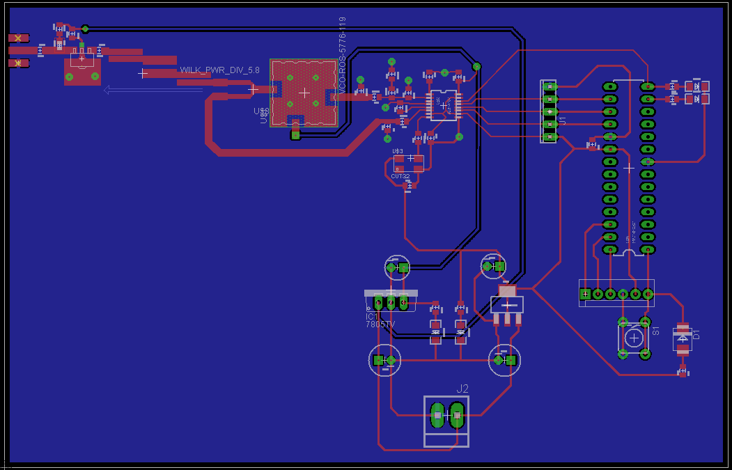
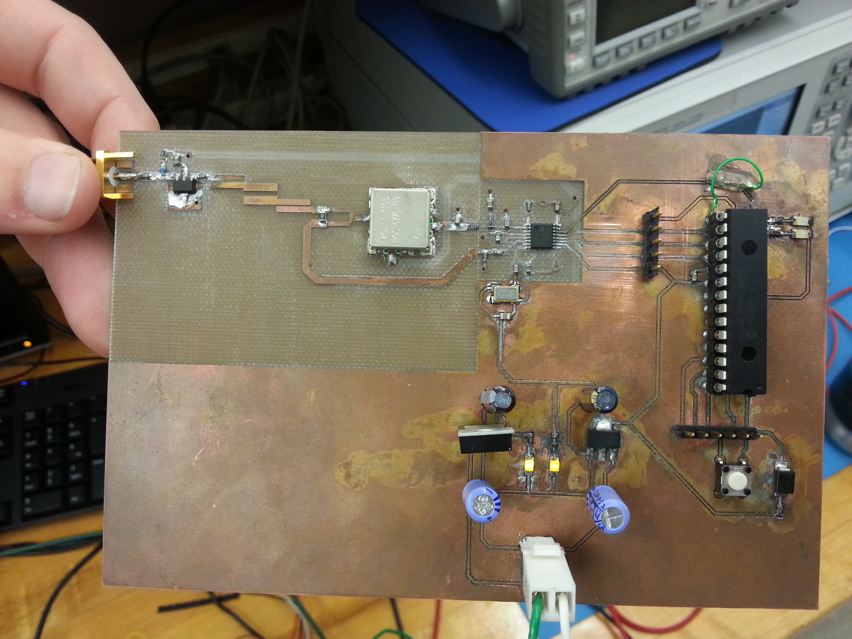
PCB Layout
The PCB layout for the signal generator was designed to be as simple as possible. The only required connectors are a 9V power connector and an SMA output for the signal. Optional programming and SPI headers are also available.
The layout was designed for a two layer board with minimal via holes. Most routing was done on the top layer with surface mount components, except for a few power traces on the bottom layer. The rest of the bottom layer was a single ground plane for both digital and RF. The board was fabricated on 31 mil FR4 with 0.5 oz copper on each side. A milling machine etched out the circuitry and drilled holes, and a chemical process was used to plate via holes for improved grounding.
Results
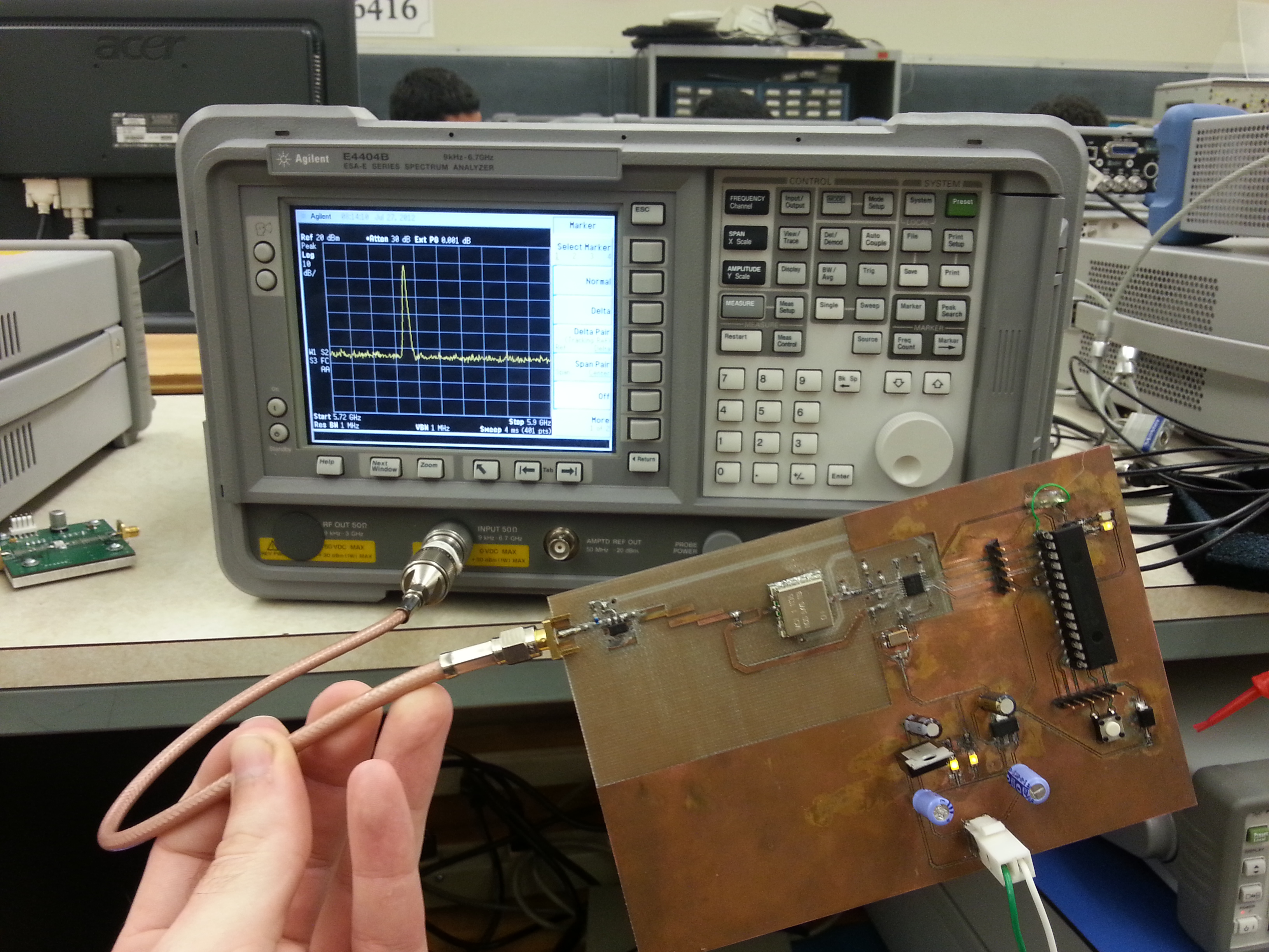
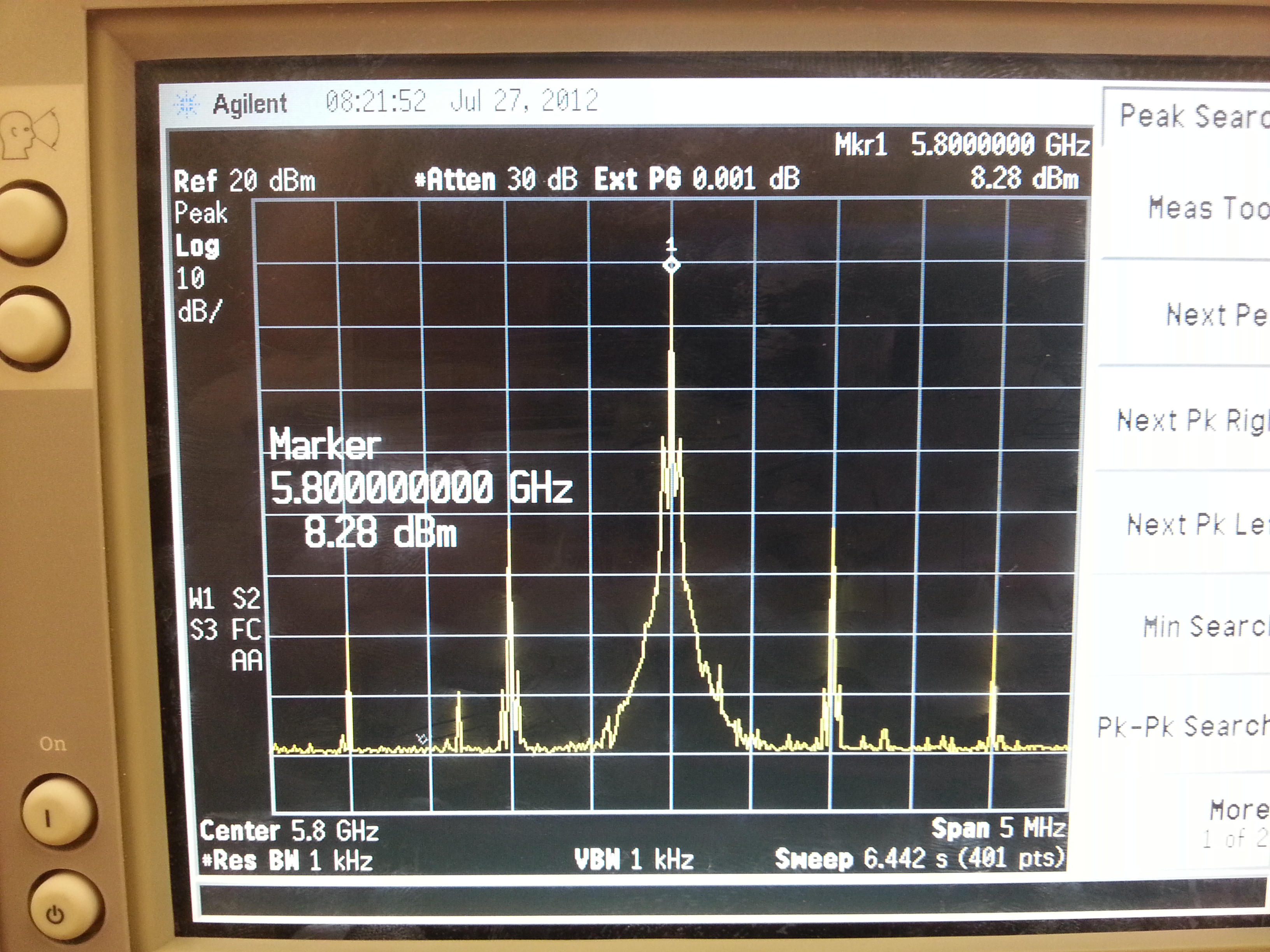
The final signal generator was a complete success and fully compliant. It hops to all 75 channels randomly and outputs about 8.6 dBm, though the output power does vary slightly depending on frequency. We were also the only group to successfully build a single board and get the PLL working properly, since the original MSP430 dev board ended up not working very well. Our approach to use the PIC was a huge benefit.
Below is a video that demonstrates the frequency hopping. You can see that roughly every .25 seconds, the sig gen moves to a new frequency. (you can ignore all the audio in the video, it's just other people working in the background)
Downloads
Project date: July 2012
Page Tools
