Sidebar
Table of Contents
Custom 2.4 GHz Mesh Sensor Network
I wanted to design a wireless sensor network in order to manage various sensors and home automation components in my new apartment. I came up with several requirements for my design:
- Node-based system with a single master node. All slave nodes (sensors) would report back to the master node. Nodes would all have the same hardware, but would behave differently depending on their configuration (stored in EEPROM). The nodes would have GPIO and TTL serial connections, so they could connect to various sensors.
- A keyfob would be used to control the system, lock/unlock doors, arm/disarm the system, etc. The keyfob should be small and very low power. Battery life should be at least a year with regular usage.
- Components should include a small PIC microcontroller (for rapid development, since it is my preferred micro family) and an RF transceiver IC that is controlled over SPI.
- Very high security. I have reverse-engineered several wireless protocols that use similar systems, so security is important to me. At minimum, some kind of challenge-response should be used for some security commands.
- Custom, lightweight protocol. I know that there are already solutions out there that don't involve re-inventing the wheel, but I wanted to design my system from scratch. I wanted to design my own wireless protocol. Sure I could have just bought some ZigBee radios and be done with it, but that's no fun! The NaliG Protocol was developed to be very small in order to reduce power consumption.
Component Selection
I have previously worked with the CC2500 from TI and the CYRF6936 from Cypress. Both are 2.4 GHz transceiver IC's (controlled by SPI, they include almost all of the RF components within the IC). I also considered the CC1101 (basically the same as CC2500, but sub-GHz) and the nRF24L01 from Nordic. The nRF24L01 is very popular with hobbyists.
I ended up selecting the Cypress CYRF6936, mostly because it supports DSSS modulation. Using DSSS is essentially an extra layer of security, since it would be very very difficult to demodulate data without the 64 bit PN code. I had also already worked with the chip, and could use my CYRF6936 Arduino dev boards for testing.
For the microcontroller, I originally selected the PIC24FV16KA301 in a TSSOP package. This family is one of the few 16-bit micros that operate at 5V. However, I eventually regretted this decision, as I ran out of flash (16k fills up quick…) and also never needed the 5V operation. I replaced most of the micros on my boards with the PIC24F32KA301, which is in the same family but has 32K of flash memory and operates at a lower voltage. The 5V I/O requirement turned out to be less important than I originally thought.
Initial Hardware Design
My idea for a keyfob was inspired by SparkFun's Nordic Fob, where they paired an Atmel ATTiny micro with an nRF24L01 to create a 2.4 GHz keyfob. I loved the idea, so I decided to make my own keyfob with the CYRF6936 and a PIC24. With a little research, I found that I could buy the same plastic keyfob enclosure from Polycase. I was able to use the Nordic Fob as a template for my design, so I could start with just the board outline, buttons (on the PCB) and battery. The board is only 2 layers, which allows me to cheaply manufacture the board in China.
Firmware Development
Firmware development was tough. Although I had worked with the CYRF6936 a little bit with a previous project, I was only doing very basic transmit and receive operations. I became intimately familiar with the CYRF6936's datasheet and user guide, although I often found Cypress's documentation either unclear or completely missing. Seriously, the user's guide (WirelessUSB LP/LPstar and PRoC LP/LPstar Technical Reference Manual) has several section headers with no text to explain some functionality (check page 48). I found that someone had done some work with the CYRF6936 and AVR's, but the level of control I need quickly exceeded those examples. The best source was Cypress's example firmware, although it was written in assembly, so it was really more of an example for when to read and write certain registers.
I spent a long time with a breadboard version of my circuit (PDIP package of the PIC24F32KA301 and my CYRF6936 Arduino dev board) so that I could use my logic analyzer and follow what was happening. Determining which registers to configure, what interrupt sources I needed, how to properly clear interrupts, etc. Eventually, I got stable connections established between two wireless modules. By “stable”, I mean that transmitted messages were reliably received, acknowledgement packets worked, the receiver wasn't receiving “garbage data” (this happened a lot in the beginning when I wasn't clearing certain interrupts/errors), and the nodes wouldn't just “stop working” after a certain amount of time (had that problem a lot too).
Once I got basic communications working, I was able to focus more on protocol development, serial command processing, and other system-level functionality (see the next section for details about the protocol implementation). As I started implementing more complex algorithms like packet relaying, I went back and optimized the CYRF6936 control code even more.
The CYRF6936 only has a 16 byte receive and transmit buffer; you can send and receive packets that are up to 256 bytes, but the firmware has to keep those buffers appropriately empty/full. Originally, I thought 16 bytes was plenty, but as the project expanded I realized that I needed much bigger packets to do more interesting things. After a few weeks of development, I was able to get large packet support working seamlessly. The TX() and RX() functions can now handle packets up to 256 bytes.
I also had trouble with making signal strength measurements. The device supports RSSI measurements, but I honestly don't think it works very well. The protocol that I developed uses “collision avoidance”. That means that before a node transmit, it listens on that frequency to hear if anyone else is transmitting. If it hears another transmitter, it will wait a small psuedo-random amount of time before trying to listen again. Once the frequency is clear, it will transmit. However, my method of listening involves making an RSSI measurement. I found that the RSSI measurement was never that accurate, so transmit collisions would happen often.
These collisions were particularly troublesome, because my original plan involved all nodes being relay nodes (re-transmit any received packet that was not addressed to itself). Without proper collision avoidance, packets were constantly being re-transmitted, relayed, colliding and re-transmitting. It's kind of a mess. I haven't solved this problem, because I beleive the problem is with the RSSI measurements. There's not much I can do. I changed my implementation, to only use one or two relay nodes, based on application. In practice, this solves the problem, but I would prefer to get it working!
Wireless Protocol
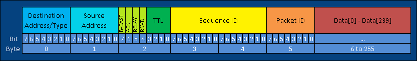
I developed the NaliG protocol for low-power packet processing. The standard packet is 6 to 255 bytes long. Packets can be any size in that range, they just need the 6 header bytes for protocol management. Although I developed this protocol specifically for these sensors with the CYRF6936, I wanted this protocol to work with any wireless IC for a small mesh network. For example, although the CYRF6936 supports auto-acknowledgement packets (greatly simplifying some firmware development), this only works node-to-node, and not in a mesh network environment. The NaliG protocol implements its own acknowledgement packets.
|
Destination Address / Type (1 byte) |
The destination field specifies a destination address or device type. If the Type Broadcast flag is not enabled, this field specifies the address of the destination node. If the Type Broadcast flag is enabled, this field is specifies the destination node type. All nodes that have a matching node type will process the packet. A node will only process a packet if:
|
|
Source Address (1 byte) |
The source address is the address of the originating source node sending the data. This field should not be changed by any relay nodes. |
|
Flags (4 bits) |
|
|
Time To Live (4 bits) |
The Time to Live is the number of relay hops remaining until the packet is discarded. When a received packet is to be relayed (the Relay flag is enabled and the destination does not match the node), the relaying node will subtract 1 from the TTL and then rebroadcast the packet. If the TTL is 0, the packet is discarded. The max TTL is 16 (0xF). |
|
Sequence ID (2 bytes) |
The sequence ID is a unique identifier for a given packet payload. The source node will generate a Sequence ID and Packet ID. If a packet must be retransmitted due to not receiving an acknowledgement, the Sequence ID will be incremented, but the Packet ID will remain the same. (See the “Relay Packets” section for more details). The sequence ID is increased for every packet that is transmitted, and doesn’t reset until it rolls over. |
|
Packet ID (1 byte) |
The Packet ID, combined with the sequence ID and Destination, creates a unique packet. The Packet ID enables receiving nodes to distinguish retransmitted packets from new packets. The sequence ID is increased for every unique packet that is transmitted (re-transmitted packets keep the same Packet ID), and doesn’t reset until it rolls over. |
|
Payload Data (0 to 249 bytes) |
The Payload Data is the actual command and data. Data bytes are optional, and the size can range from 0 to 249 bytes. In most cases, the first data byte will be interpreted as the command for the current packet. Usually, only acknowledgement packets will not have payload data. |
Packet Cache
In order to ensure that re-transmitted packets aren’t processed multiple times, all nodes should maintain a Least Recently Used (LRU) packet cache of at least 10 packets. The cache entry is an unsigned long (4 bytes) and contains the concatenation of the (MSB) Destination, Sequence ID and Packet ID (LSB) fields. Only packets that have been relayed or accepted (matching Destination) by the node should be added to the packet cache.
If the packet cache is full when another packet must be added, the oldest packet should be removed so that the newer packet can be added. If a packet is received that completely matches an entry in the packet cache, the packet should be discarded. The entry in the packet cache should be moved to the top of the cache. If a packet is received that partially matches an entry in the packet cache (packet ID matches, but different sequence ID), the node should send an acknowledgement packet back to the origin, but should not actually process the packet. The entry in the packet cache should also be moved to the top of the cache.
ACK Packets
An “acknowledgement packet” is a packet with the ACK flag set. Ack packets should be 6 bytes long (extra bytes will be ignored). They do not have any data payload bytes. The ACK packets replace the CYRF6936’s auto-ack packets so that they operate in a mesh environment. ACK packets should be relayed like all other packets.
Relay Packets
Packet relaying is used to get extended range for transmission by allowing other nodes to retransmit data. The source node allows packet relay by enabling the Relay flag for a packet. If the source node must retransmit a packet (due to not receiving an acknowledgement from the first transmission) the source node should send another packet with the same Packet ID, but increment the sequence ID so that other nodes will still retransmit it (and not discard the packet due to the packet cache).
Functionality Overview
I designed these wireless modules primarily for a security system. As such, I knew that I would be moving, re-purposing, and changing the behavior of the modules often. So, I wanted the modules to be relatively “dumb”, and have most of the system intelligence come from the master node(s).
Each node uses a small amount of EEPROM on the PIC24 to store the device address, device type, and device settings. Settings include features such as blink-alive for the LED, packet relay, RF front end config, and other features. Device addresses are 0x01 through 0xFD. 0x00 is invalid, 0xFF is broadcast, and 0xFE is “not configured”. Devices that power up with any of these invalid address are configured as “not configured”, and blink white 3 times when they power up. These “not configured” devices will still follow most commands.
When a configured node powers up, it might make some configuration changes specific to that device type, such as change I/O pin states or send a serial command. They will also send an “I'm alive!” message to the master node. Keyfobs will automatically power down their radios and go into idle mode, waiting for a button to be pressed.
After power-up, all regular nodes (anything but a keyfob) will listen for RF commands. Some nodes (such as EnviroNode or ControlPanel) will also wait for serial commands, and some will wait for GPIO pin changes (motion sensors, door sensors). There is no intelligence with these nodes - they simply send packets over RF when required to (depending on their device type), or send out serial commands when commanded to by the master.
For example, audio nodes do absolutely nothing while idle. When they receive a command to play an audio file, they send the appropriate command over serial. Okay, I lied, there is some intelligence - if the SerialMP3 module doesn't respond to the command, the node will report an error to the master.
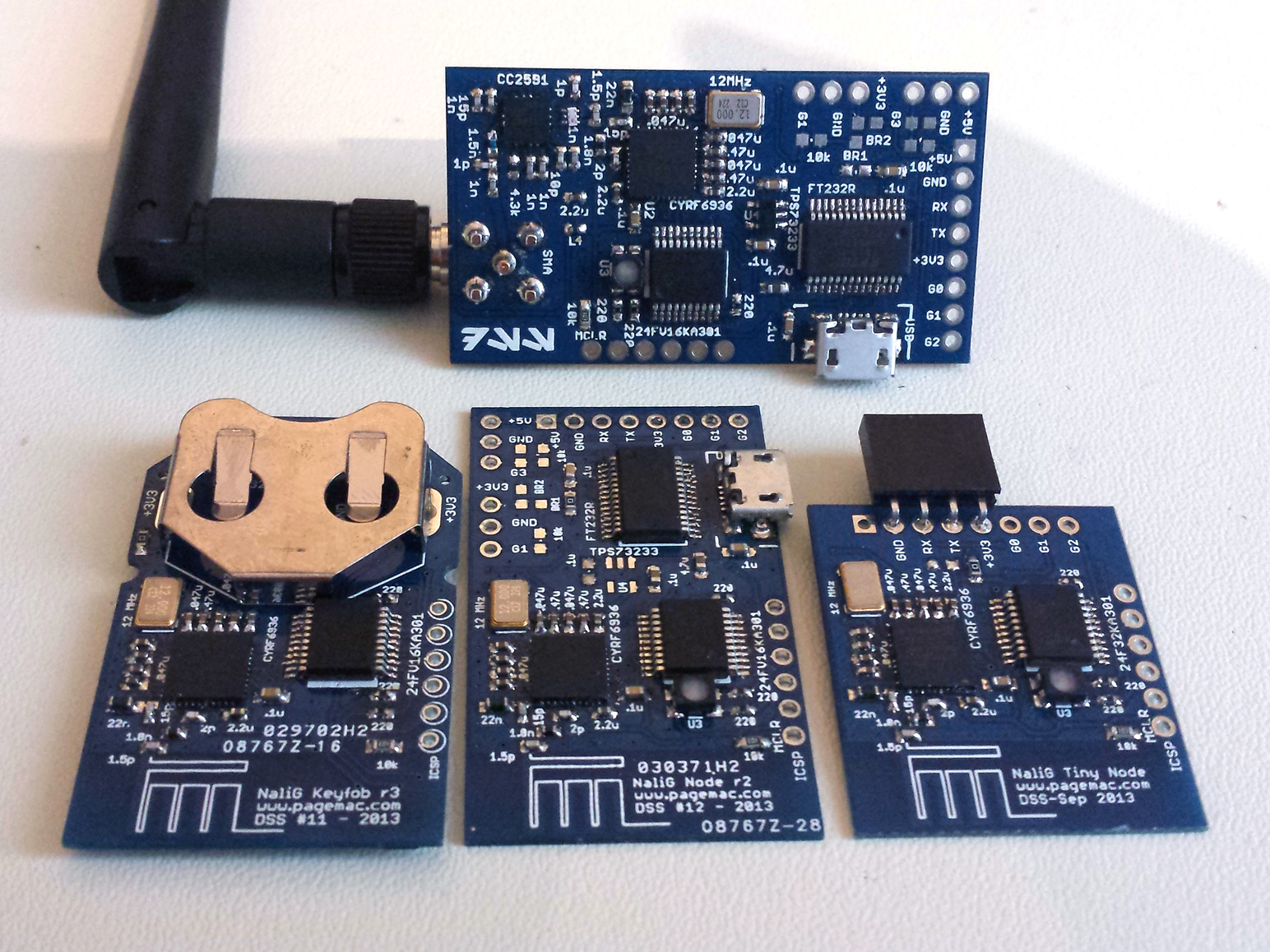
Module Hardware
As I developed the hardware for use with my security system, I ended up making several hardware variations of the wireless modules. All modules share the PIC24F32KA301 microcontroller, RGB LED, CYRF6936 wireless IC, and passive components to match the RF input/output to 50 ohms.
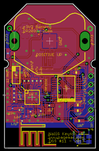
Keyfob
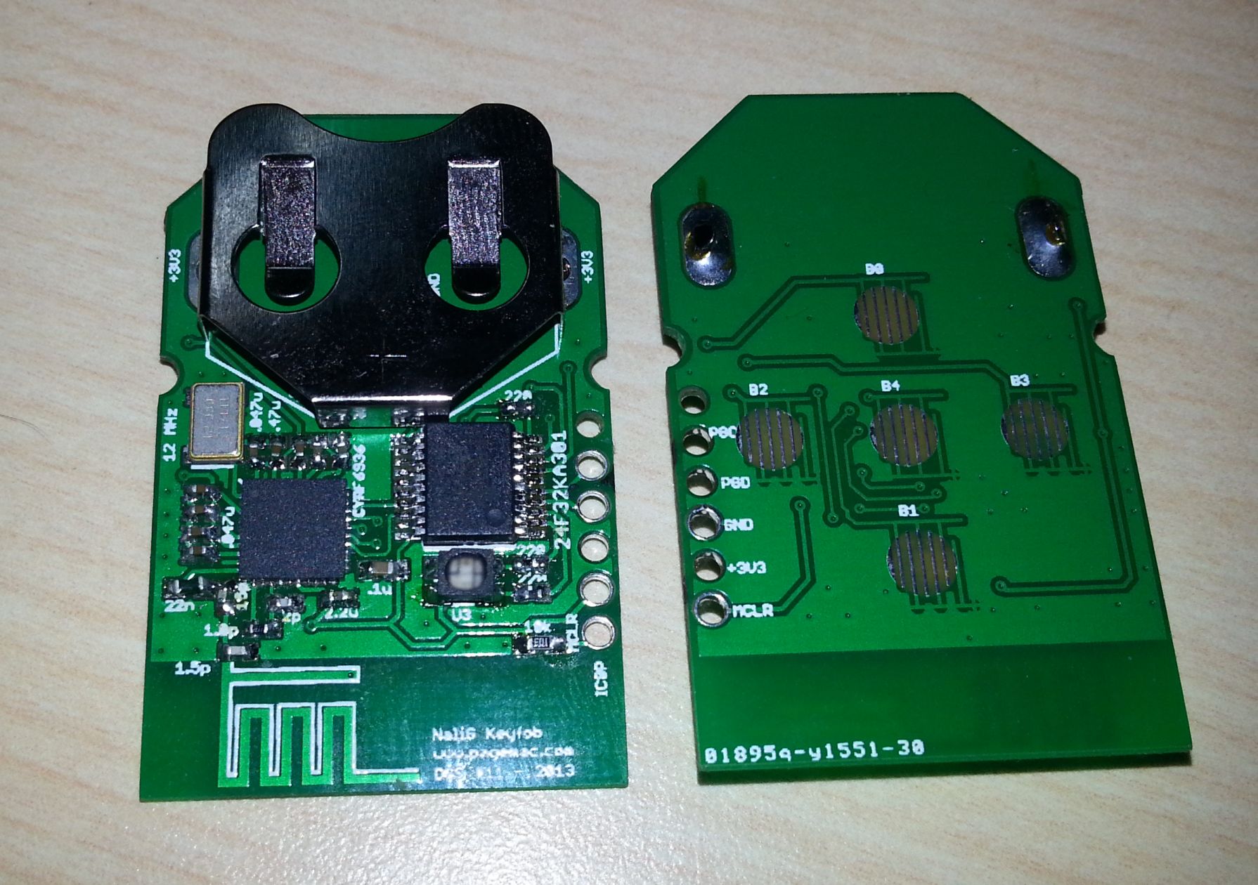

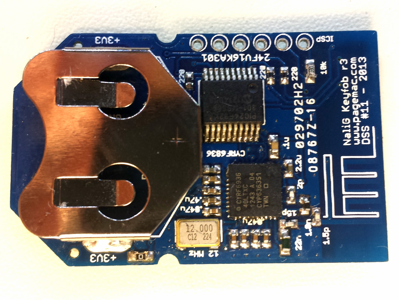
As stated above, the keyfob was based on and inspired by SparkFun's Nordic Fob. This was the first module developed for the system, and initial testing was done with the keyfob and the CYRF6936 Arduino module.
The first revision worked quite well, and the basic layout didn't change. However, in rev 2 I moved the RGB LED to the back of the board, which is the same side as the buttons and lets you see the LED when you are pushing buttons. On the 3rd and 4th revisions, I added a TPS62733 power regulator in order to get the battery to last longer - the rev 1 boards are directly powered by a CR2032 lithium coin cell battery. This actually never really worked out, since the TPS62733 outputs 2.1 V, which is just below the CYRF6936's operating voltage. It actually does work and increases battery life, but as you would expect, the radio doesn't perform as well.
I spent a lot of time trying to maximize the battery life of this device. There is a lot of firmware devoted to power saving - the wireless chip is completely turned off except when needed, and power transmit levels are slowly ramped up until a response is heard. Although the CYRF6936 is supposed to be able to draw as little as 1uA, I have yet to get the device to draw less than 25uA in idle mode. I tried everything to get that as low as possible, but eventually gave up - with that current draw, the battery should still last up to a year.
The keyfob PCB is 1.06“ x 1.69”. This board was made in December 2012.
Basic Node
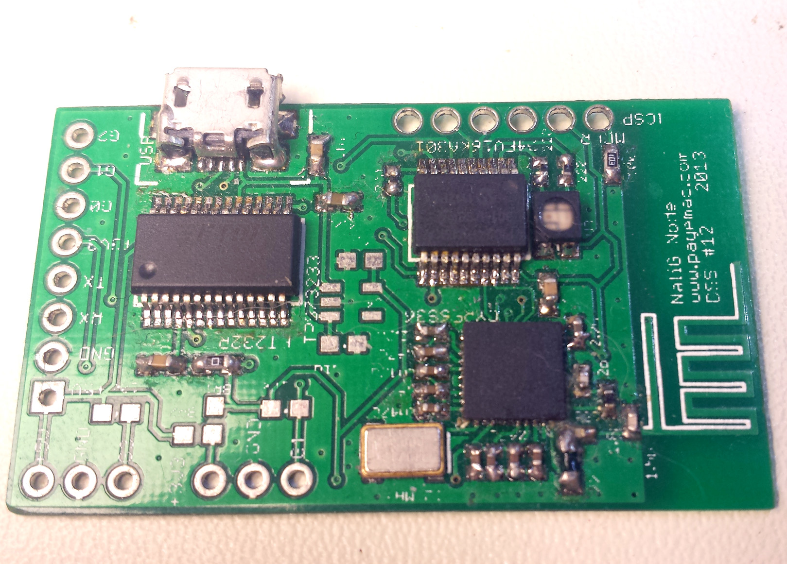

The basic Nalig Node was intended to be as universal as possible. In addition to the components found on the keyfob (minus the buttons), it has a PCB trace antenna, an 8-pin header for power and/or I/O, two 3-pin headers for additional I/O, a micro USB connector for power and/or data, an FT232RL for USB serial support, and a SOT-23 3.3V LDO power regulator.
- The PCB antenna is cheaper (free, actually, since it is part of the PCB) and smaller than an SMA antenna, and probably just barely worse in performance than a chip antenna.
- 8-pin header has +5V, +3.3V, serial, and 3 I/O pins. The pinout matches the Raspberry Pi, so it can easily be connected.
- 3-pin headers were made with motion sensors in mind, so they have a matching pinout. There's also a spot for a pull-up resistor on the data line.
- The micro USB connector is the primary way to provide power. This is a convenient way to power nodes, since I have a ton of USB chargers and cables.
- The FT232RL provides easy USB to UART serial. This is mostly only used for debugging, computer-controlled nodes, and sniffer nodes.
- The 3.3V LDO regulator is required for boards that are powered by 5V. Optionally, there's also a solder bridge to use the FT232RL's 3.3V regulator instead.
- Most nodes don't have all of these features populated. I wanted to be able to mix-and-match components as needed, and build nodes for specific tasks.
The basic node PCB is 1.06“ x 1.78”. This board was made in March 2013.
Tiny Node
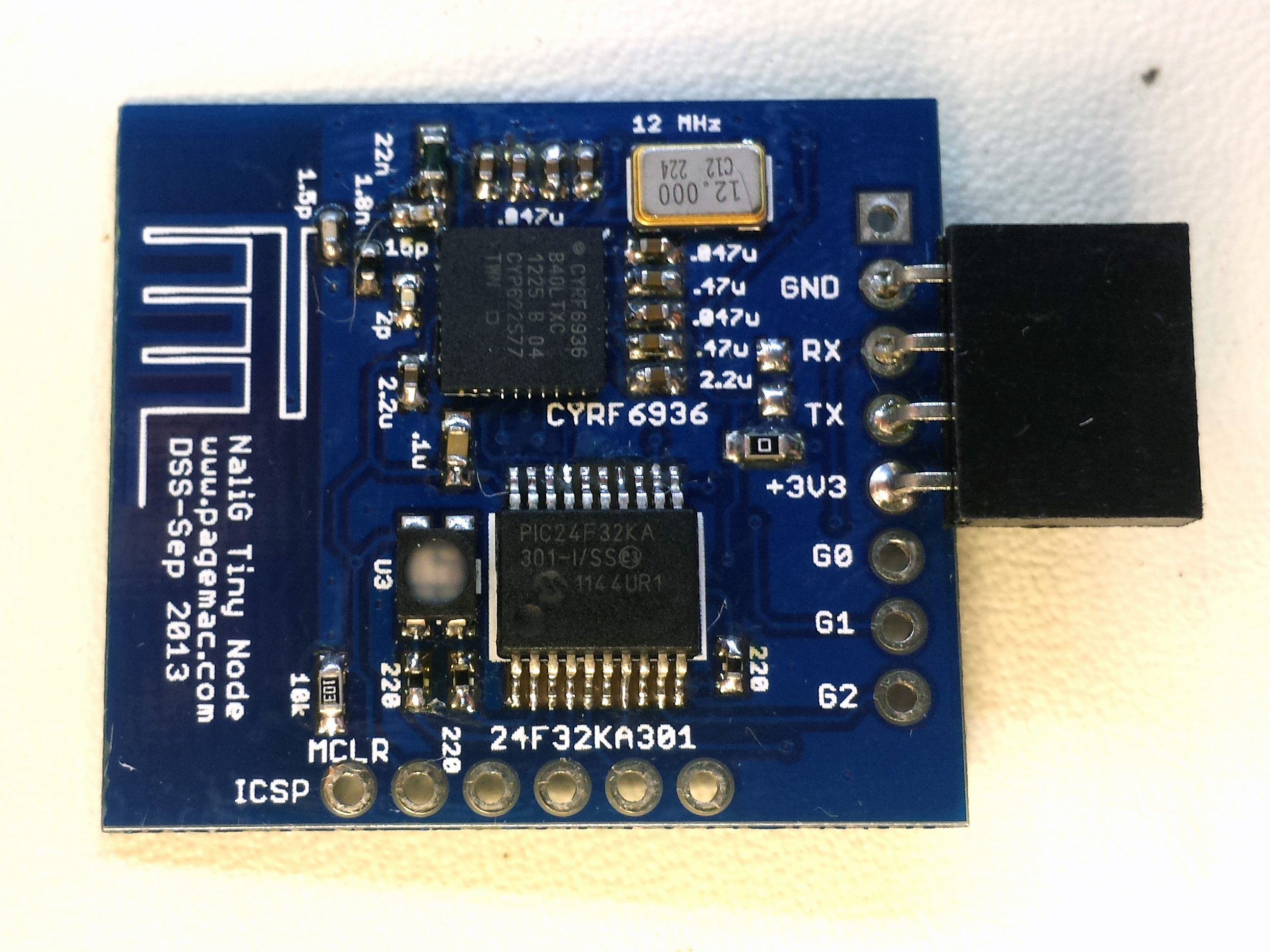
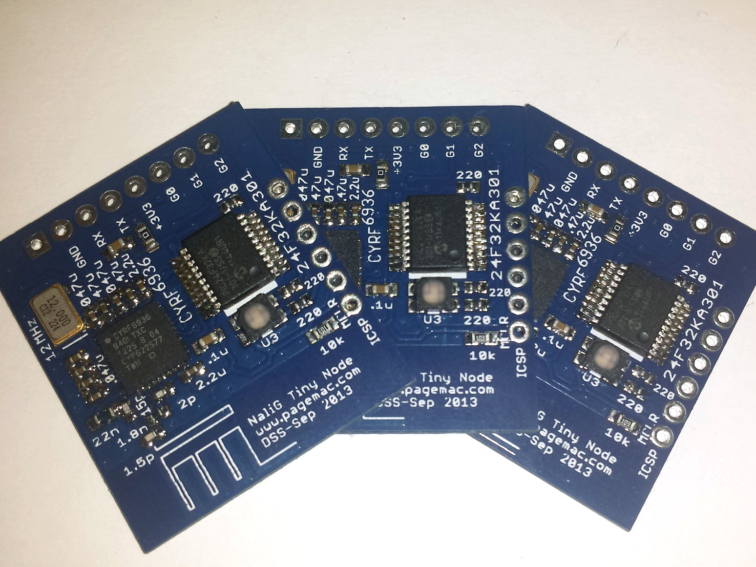
I made the Tiny Node for applications that only required the 8-pin header from the Basic Node. I found that most applications only needed this header, and half of the Basic Node would be left un-populated. So, I made the Tiny Node, which is about half the size of the Basic Node, and only has the 8-pin header. Since there is no voltage regulator, this board must be powered by 3.3V. I use this node mostly with the serialMP3, EnviroNode, or LED Panel.
I had originally planned for the Basic Node to be my most-used node, but I actually use the Tiny Node the most. I like that it is smaller. It's also handy for remotely controlling TTL serial objects, such as robots, in serial bridge mode.
The tine node PCB is 1.06“ x 1.21”. This board was made in September 2013.
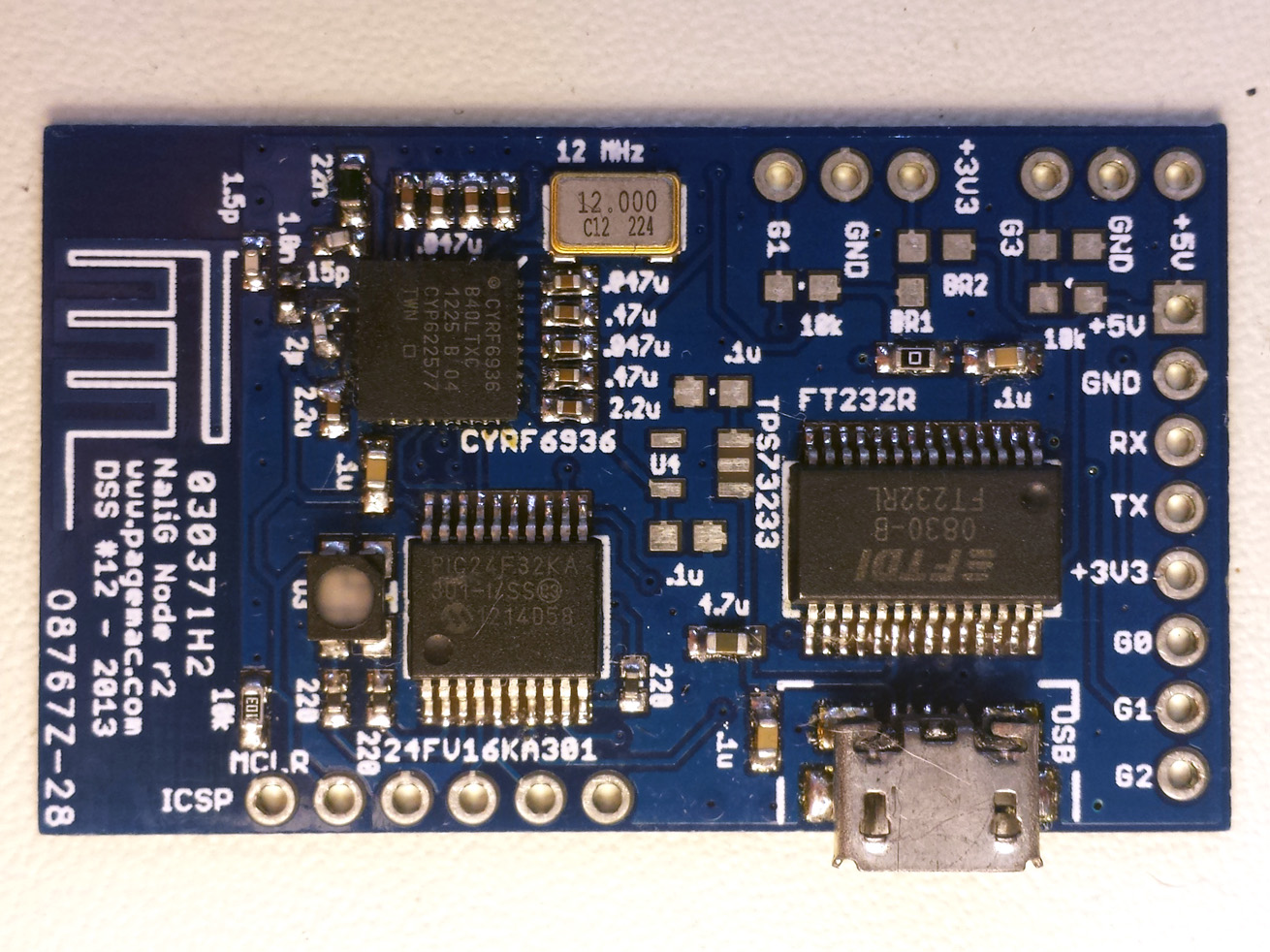
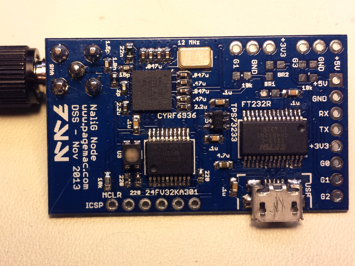
Super Node

The Super Node was my attempt to create a more powerful wireless node. I wanted to use the CC2591 RF front end from Texas Instruments to increase the range of certain nodes, particularly the master node. Unfortunately, there is no easy way to integrate TI's front end modules with non-TI transceivers. TI provides application notes and example schematics / layouts to integrate them with most of TI's line of 2.4 GHz transceivers, but they don't provide key technical details (such as the input/output impedances at various frequencies/power levels) to design your own circuits. The CYRF6936 and CC2591 both use differential RF connections, but without impedance information, I couldn't design a proper matching network to connect them together.
However, the other nodes already match the CYRF6936 to 50 ohms, and one of TI's application nodes match the CC2591 to 50 ohms. I decided to put these together and see if it would work. Although it would add some loss and extra components (and take up valuable board space!), it should work.
Unfortunately, after spending a couple weeks designing, assembling, and writing a little more code for this board, I couldn't get it to work as well as I would like. I was able to get about 13 dBm of output power (theoretically could have been up to 22 dBm), but I lost a significant amount of receive sensitivity. The board was basically deaf - it could not hear nodes that were further than a few feet away.
It was a long shot to begin with; there were too many constraints on the design. The board had to be only 2 layers (which made routing difficult, and is generally a bad idea for anything but basic RF designs), thick 50 ohm microstrips, and other issues. Somehow I still maintained a pretty good ground plane. I tried maintain roughly the same layout as the Basic Node AND be less than 5cm in length (to reduce manufacturing costs), and as a result the RF trace from the CC2591 to the SMA connector curves and travels a few cm. Probably a fair amount of loss there. The 50 ohm match also probably introduced some loss.
Oh well!
The Super Node PCB is 1.06“ x 1.96”. This board was made in October 2013.
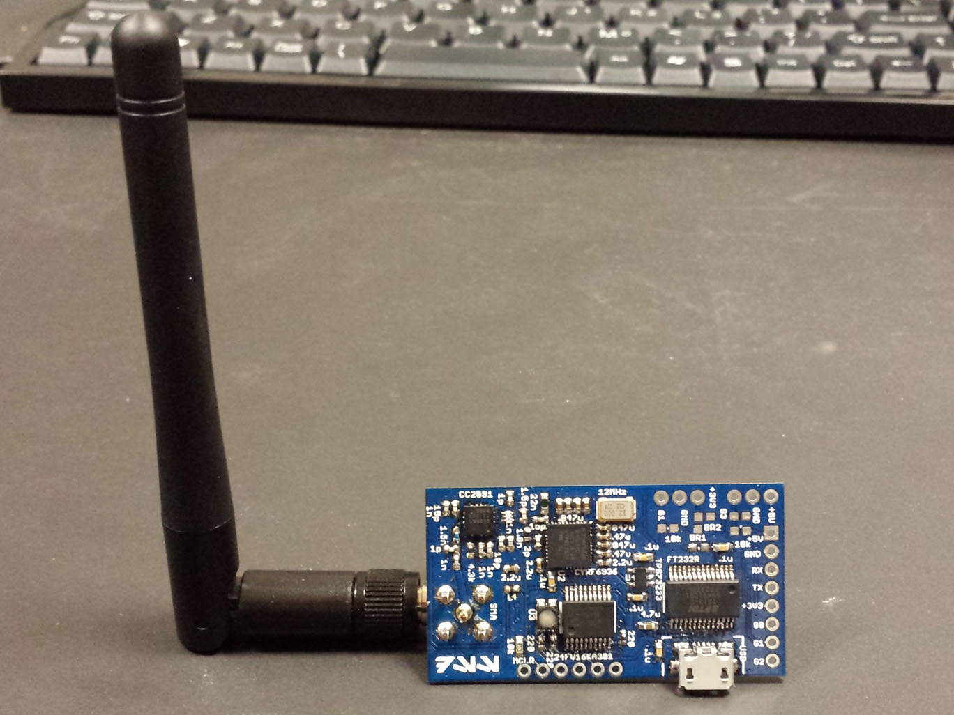
Antenna Node

After failing to get the Super Node to work properly, I decided for a simpler approach to increase range: ditch the PCB trace antenna, and add an SMA connector so I could use an antenna with actual gain. According to Cypress's application note (AN48610), the PCB's antenna's gain is around .7 dBi, give or take a dB. I figured that if I replace the PCB antenna with an SMA connector, I could add an antenna (like this one) with more gain, thus increasing sensitivity and range of the system. Since the input to the PCB antenna is about 50 ohms, I didn't have to change anything else on the board. I installed the through-hole SMA connector on the bottom, to reduce impedance mismatches that might be caused from the connector going over the strip line.
This node works great! I didn't do any formal testing, but a few informal tests showed greater range and reduced packet loss when operating within the mesh network.
The antenna node PCB is 1.06“ x 1.82”. This board was made in November 2013.
Downloads
Feel free to contact me if you have any questions trying to re-implement any of this design.
Page Tools
